
JDI's new strategy. Focus on creating value by leveraging technology that claims to be the best in the world
On June 22, Japan Display (hereinafter JDI) held a “METAGROWTH 2026” briefing in Tokyo to introduce the company's technologies to journalists.
The company is currently developing a number of new technologies and rebuilding its business model on this basis. What we can see is what will happen to next-generation screens.
I would like to explain what it is.
“Hinomaru” JDI aims to be the “arm of the display world”
First, I would like to briefly review JDI.
JDI was established in September 2011. The company was originally formed by combining the small and medium-sized display panel manufacturing businesses of Sony, Toshiba and Hitachi with Panasonic LCD. Panasonic LCD itself is based on “IPS Alpha technology”, which was a joint venture between Panasonic, Toshiba and Hitachi. So it would be more appropriate to call it “a company that brings together the LCD display businesses of major home appliance manufacturers.” other than Sharp.” unknown.
The goal was to consolidate and expand each company's LCD panel business, which had become difficult due to pressure from Korean and Chinese competitors, and compete as “Japanese Flag LCD”.
This initiative was therefore not a success and the financial situation of the company remained difficult. As demand for iPhone LCD panels slows, profits will slow further. They found themselves in a very difficult financial situation.
From documents published by JDI. Sales of smartphone panels, which amounted to 312.9 billion yen in 2019, will drop to 77 billion yen in 2021.
The share of the smartphone sector, which was 80% in FY2020, is expected to fall to less than 10% by FY2026.
The company's capital and management structure have undergone extremely complex changes, including the impact of the accounting fraud incident, but as this is not the main topic of this article, I will omit this point . In October 2020, the company sold its factory in Hakusan City, Ishikawa Prefecture to Sharp and Apple, and has been working for two years to stabilize management under the new system.
What are the measures to achieve this?
Scott Caron, president and CEO of JDI, proposes two directions.
Scott Caron, President and CEO of JDI
The first consists of diversifying its sources of income, too concentrated on smartphones, which constitute Apple's only activity. The second concerns licensing measures that exploit technology.
“Our company has excellent human resources and high technological capabilities. Therefore, since I became CEO two years ago, I have helped the company meet the challenge of creating the first and best technology in the world that no other company could create.”
“Our goal is Arm for the display industry”
CEO Caron says so.
Conversely, this means that even though they possess some of the most advanced technological capabilities in the world, they have recognized that they cannot participate in the production of the massive display industry with their capital alone.
Mass production of displays is important. This requires huge production equipment, and the demand to operate the production equipment is also huge.
JDI failed to achieve such capital and sales development measures. However, if they adopt a strategy of actively recruiting partners, this becomes another company's domain.
However, to achieve this, we must demonstrate that we are of great value. Furthermore, even if it were possible, it would take a long time before it would have a real impact, including in terms of production planning.
Therefore, licensing is currently not considered in the compensation plan.
Promote innovations in automobiles, HMDs, etc. with transparent screens
In short, the reason why you are leveraging your company's technological assets now is also for your future projects.
It is true that the technologies presented by the company are all interesting.
The “Rælclear” transparent screen was often featured on television and other media.
JDI “Rælclear” 20-inch LCD “clear as glass”
The real “Rælclear” machine exhibited on site. We see that the transparency is very high.
As you can see, it is a transparent screen. Although it is essentially a liquid crystal display, it is made of a highly transparent material and has a mechanism that allows content to be read from both sides, allowing it to be viewed from both sides with the display between the two. With other companies you can only see it from one side and the transparency is not high, so it is difficult to use it in the same way as Rælclear.
Features and structure of Rælclear. There are many elements that are not found in transparent screens from other companies.
This is a typical example of a “one of a kind” device.
Non-smartphone applications expected to grow include automobiles and HMDs (head-mounted displays).
Demand forecast for automotive billboards. Flexibility in the number and shape of panels will become important for high-end products and electric vehicles.
Probably the easiest to understand is HMDs.
In fact, JDI is already the leading manufacturer of LCD panels for HMD, and in 2021, JDI products account for almost 40% of the market.
The demand for HMD is expected to increase in the future. In 2021, JDI already holds a 40% share in this area
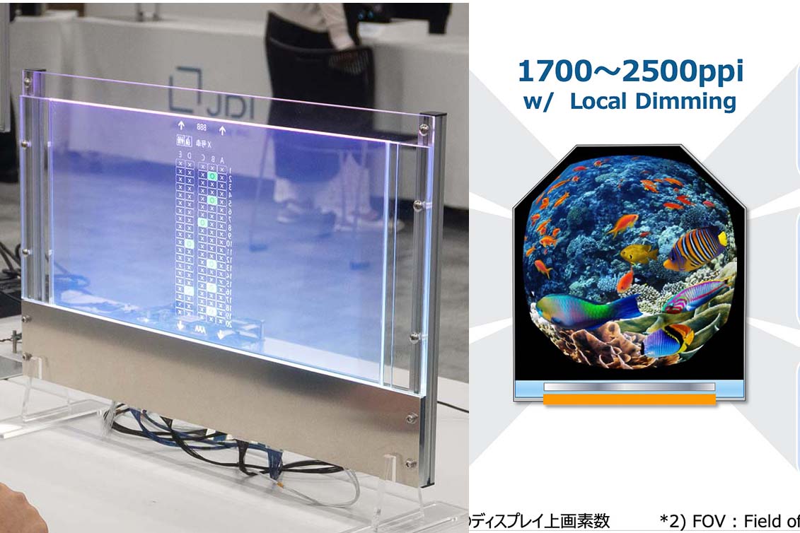
Resolution is especially important for HMDs, and JDI is making products with a resolution of 1,201 ppi (pixel per inch) in 2021, and will almost double that to 2,000 ppi in 2025. I also saw the prototype, and I feel like the resolution is pretty close to reality.
A look at the displays JDI produces for HMDs and the products it plans to develop by 2025. Resolution increases significantly
In the future, 2500 ppi HDR compatible devices will also be developed, with the principle of using a “pancake lens” suitable for small devices.
In the future, a single eye will have a resolution of 4K x 4K and the contrast will scale up to 100,000:1.
Furthermore, regarding lenses, instead of classic lenses, we are also developing flat and thin lenses using holograms. Although the technology is different, the idea is the same as that used in Holocake 2, a device that Meta has teased as a “future direction.”
A “holographic optical system” type lens currently under development. It's hard to tell in the photo, but it's flat and thin.
“HMO” and “eLEAP” on which JDI is betting the future
Two technologies have greater potential than these: “HMO” and “eLEAP”.
HMO is a technology in an area called “backplane side” that drives display elements. It contributes to higher definition, lower power consumption and larger screens.
HMO technology is linked to the TFT surface which exploits the pixels, allowing pixels to operate with high resolution and low power consumption.
eLEAP is even more revolutionary. This technology is aimed at organic ELs, but according to a JDI explainer, it is “advantageous in all respects over existing organic ELs” and is a technology that can produce superior products.
JDI Establishes “eLEAP” Mass Production Technology That “Exceeds All Characteristics of Existing Biological ELs”
eLEAP is a technology that configures pixels. Since no metal mask for vapor deposition is used, the brightness and lifespan are significantly extended.
The key point is that the pixels are coated by photolithography and the “metal vapor deposition mask” used in current organic EL manufacturing is not used.
Most current organic electroluminescent devices deposit red, green, and blue light emitters through a metal mask. It's like a template with holes in it, and after three deposits of red, green and blue, the metal mask is washed with an organic solvent and reused.
Since the coating is applied to the holes, the area that cannot be covered is surprisingly large, with only 28% of the pixels actually glowing.
However, eLEAP does not use a metal mask for vapor deposition, but instead uses photolithography technology to apply one color at a time. As a result, a process of cleaning the metal mask becomes unnecessary. This will reduce plant area, reduce labor time and eliminate the need for water containing solvents used in the cleaning process, thereby significantly reducing environmental impact.
As the metal vapor deposition mask does not need to be cleaned, the environmental impact of manufacturing is significantly reduced.
In addition, since the light emitting area becomes significantly wider, the brightness can be significantly increased using the same amount of power, and conversely, the power can be reduced to extend the lifespan, reduce the energy consumption and avoid burns. By combining the HMO mentioned above, it is possible to further improve the resolution and reduce power consumption.
Initially, the company is targeting the “PC and car displays” market with sizes ranging from 10 inches to 30 inches, but the company says it can be used in a wide range of applications including TVs, smartphones and larger HMDs.
Another feature of eLEAP is that it can be used with a wide range of screen sizes.
Unfortunately, no product prototypes were displayed on site, so it was not possible to verify the quality of the image. However, it is currently in prototype production and development is progressing with the goal of mass production around 2024.
On the other hand, although eLEAP and HMO are promising technologies, the cost benefits will only be realized if they are adopted by manufacturers producing in large-scale factories. This is why JDI is promoting its partnership strategy this time.
I hope they can find a good partner to take advantage of the company's excellent technology and make products using it. And these partners will likely no longer be Japanese companies, but large-cap manufacturers from countries like China, South Korea and the United States.
Technology briefing “METAGROWTH 2026”